Introduction
In the rapidly evolving world of electronics, custom printed circuit board design plays a crucial role in bringing innovative products to life. From consumer gadgets to industrial machinery, PCBs are the backbone of modern electronic devices. Creating a custom PCB requires precision, technical know-how, and a clear understanding of both design and manufacturing processes. This guide will take you through the essentials of designing high-quality, reliable PCBs, ensuring your electronic project achieves its full potential.
Understanding Custom Printed Circuit Board Design
What is a Custom Printed Circuit Board?
A printed circuit board (PCB) is a platform that mechanically supports and electrically connects electronic components using conductive pathways, or traces. A custom PCB is tailored specifically for a particular device or function, allowing designers to optimize space, performance, and functionality.
Benefits of Custom PCB Design
- Optimized Performance: Custom PCBs allow precise placement of components to reduce interference and improve signal integrity.
- Space Efficiency: Tailored layouts help fit complex circuits into smaller devices.
- Reduced Production Costs: Well-planned designs minimize material waste and simplify assembly.
- Enhanced Reliability: Custom PCBs undergo rigorous testing to ensure durability and long-term performance.
The Custom PCB Design Process
Conceptualization
The design process starts with a clear understanding of the device’s functionality and requirements. Engineers outline specifications, component lists, and power needs. Sketching initial layouts helps visualize the placement of major components.
Schematic Design
A schematic is a blueprint that illustrates the electrical connections between components. Engineers use software like Altium Designer, Eagle, or KiCad to create schematics, ensuring that all components are properly connected and functional.
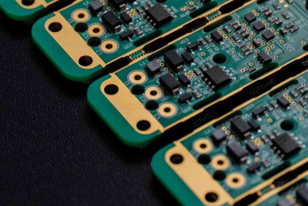
PCB Layout
Component Placement
Optimal component placement is crucial for reducing noise, minimizing trace lengths, and ensuring thermal management. Critical components, such as microcontrollers and high-frequency circuits, are positioned strategically.
Routing and Trace Design
Traces must be designed to handle the expected current and minimize electromagnetic interference. Multilayer boards allow for more complex routing and improved signal integrity.
Design Verification
Before manufacturing, the design is checked using Design Rule Checks (DRC) and Electrical Rule Checks (ERC) to catch errors. Simulation tools can predict performance issues like voltage drops or heat accumulation.
Prototype Manufacturing
Once the design is finalized, a prototype is created. This allows engineers to test functionality, signal integrity, and thermal performance. Any necessary adjustments are made before full-scale production.
Production and Assembly
After successful prototyping, the PCB goes into mass production. Automated assembly processes like Surface Mount Technology (SMT) and Through-Hole Technology (THT) ensure consistent quality.
Advanced Considerations in PCB Design
Thermal Management
Overheating can damage components. Designers must consider heat sinks, thermal vias, and proper spacing to dissipate heat effectively.
Signal Integrity
High-speed circuits require careful attention to trace impedance, crosstalk, and grounding. Using multilayer boards and differential pairs can improve signal performance.
Material Selection
Choosing the right substrate, copper thickness, and solder mask affects durability, thermal conductivity, and electrical performance.
Regulatory Compliance
Custom PCBs must meet industry standards, such as IPC standards or RoHS compliance, to ensure safety and market acceptance.
Custom PCB Design Tools and Software
- Altium Designer: Advanced routing and 3D modeling.
- Eagle: User-friendly and widely supported.
- KiCad: Open-source, ideal for cost-conscious projects.
- OrCAD: Comprehensive simulation and design features.
Learning Resources
For those interested in the printing side of PCB components and packaging, exploring print & finishing insights can provide valuable tips on material handling and production techniques.
Related Applications
- Consumer electronics
- Industrial automation
- Medical devices
- Automotive electronics
Custom Packaging for PCBs
Protecting your PCB during shipping and storage is essential. Consider using Custom Packaging to ensure your boards arrive safely and maintain their integrity. Packaging solutions tailored to your PCB design can prevent damage from static, moisture, and mechanical shocks.
Choosing the Right PCB Manufacturer
Selecting a reliable PCB manufacturer is critical for successful production. Evaluate their:
- Manufacturing capabilities (multilayer, flexible, rigid-flex boards)
- Quality certifications (ISO, IPC)
- Turnaround time and support
- Cost-effectiveness
Visiting the facility, like checking Buddy Packaging Location, helps verify their processes and quality standards.
A successful custom printed circuit board design requires a balance of creativity, technical skill, and attention to detail. From conceptualization to production, every step impacts the performance and reliability of the final product. By following best practices, using the right tools, and working with reputable manufacturers, you can ensure your PCB meets both functional and quality expectations.
FAQs
What is the difference between a custom PCB and a standard PCB?
A custom PCB is designed for a specific application, allowing for optimized layout, size, and performance, whereas a standard PCB follows generic specifications.
How long does it take to design a custom PCB?
The design timeline varies by complexity. Simple boards may take a few days, while complex multilayer boards can take several weeks.
Can I manufacture a custom PCB at home?
While basic PCBs can be made at home using DIY methods, professional-quality custom PCBs require precise manufacturing equipment.
What software is best for PCB design?
Popular software includes Altium Designer, Eagle, KiCad, and OrCAD, each offering different levels of functionality depending on project needs.
How do I ensure my PCB is durable?
Proper material selection, thermal management, and design verification are key to creating a durable and reliable PCB.